
Summary
In this project we develop a quantum interface between microwave and optical photons as a key enabling technology of a hybrid quantum network. In such a network, the robust optical photons carry quantum information through optical fibres over long distances, while superconducting microwave circuits protected from thermal photon noise by the low temperature environment of a dilution refrigerator function as quantum nodes, providing memory, processing and routing capability. Our work includes developing an integrated, microfabricated device that interfaces the fragile microwave photons and with optical photons through either individual or ensembles of three-level solid-state quantum emitters, such as nitrogen vacancy (NV) centers in diamonds. In addition, we are developing novel quantum memory and repeater designs. Here the device itself could serve as an optical quantum memory, storing information in the ground states where we may perform quantum control via a microwave circuit. It could also serve as a specialized quantum node. Entangling operations between remote superconducting circuits can be performed for repeater operation. Finally, we will also develop an efficient microwave photon detector that works by converting microwave photons into optical photons, which can then be efficiently detected with existing technology.
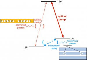
Figure 1. Microwave to optical conversion with a three level quantum emitter coupled to a microwave stripline cavity and an optical, e.g. a photonic-crystal, cavity: A microwave photon couples the two ground states |g> and |s> of a three-level quantum emitter with the help of the microwave cavity. The conversion is then completed through an optical pump and an enhanced emission into optical cavity coupled to the transition between the excited state |e> and the ground state |g>.
Related Content

Quantum Computational Resources in the Presence of Symmetry
Summary Fault-tolerance is essential to the performance of quantum technologies, but known schemes are extremely resource intensive. Thus, improving existing schemes or inventing new schemes is of central importance. This joint project is based on the realization that fault-tolerance schemes make use of symmetries in fundamental ways, and that studying the problem of fault tolerance […]
March 13, 2019

Quantum Information Processing with Molecular Lattices
The aim of the work is to develop theoretical tools to simulate and predict the behaviour of a one-dimensional chain of trapped dipolar molecules and to study the nature of entanglement as a design resource.
June 1, 2017

Hybrid Quantum Materials towards Topological Quantum Computing
Summary Proximity engineered hybrid materials have shown promise for topological quantum information processing. This form of quantum computing provides a stable, error-tolerant approach for building scalable quantum information processors. Topological quantum computing relies on braiding non-Abelian particles, such as Majorana fermions, which do not exist in nature. One can however use materials engineering to […]
December 8, 2018

Quantum State Tomography with Machine Learning
Summary An important challenge in building a quantum computer is quantifying the level of control obtained in the preparation of a quantum state. The state of a quantum device is characterized from experimental measurements, using a procedure known as tomography. Exact tomography requires a vast amount of computer resources, making it prohibitive for quantum […]
June 6, 2018