
Photonic quantum processors based on integrated quantum photonic circuits require entangled photon pairs to perform quantum computations. However, current state-of-the-art technologies utilize probabilistic entangled photon sources with limited pair-extraction efficiencies, negatively affecting the computation speed. This project aims to boost the speed of on-chip quantum operations by using bright, on-demand entangled photon sources with an extraction efficiency of more than two orders of magnitude higher than the existing state-of-the-art technology based on probabilistic photon sources. Our novel photon source will be developed by embedding quantum dots in tapered nanowire waveguides and surrounding them with a microcavity that accommodates entangled photons. This setup will produce bright, highly entangled photon pairs at a specified rate in a well-defined time interval, with high single-photon purity, pair extraction efficiency, photon indistinguishability, and entanglement fidelity. The tapered geometry of the nanowire allows for simple and efficient coupling of the produced photons into a low-loss optical fibre. This will enable the quantum dot sources to operate in a low-temperature cryostat, while the integrated photonic circuits operate at room temperature. Through fibre optic cables, the photons will be inserted into the integrated photonic circuit using custom-designed components such as grating couplers and edge couplers. This modular approach will be used to implement a vital protocol known as entanglement swapping, which is critical for large-scale quantum computing. Two core operations, a Bell-state measurement and quantum state tomography, will be performed by the integrated photonic circuits. The result of the procedure will be that two remote integrated photonic circuits will share entanglement. This novel quantum light source technology combined with integrated quantum photonic circuits will boost the speed, efficiency, and scalability of quantum operations compared to the current state-of-the-art system. Thus, this project will develop critical components of quantum photonic technologies that can pave the way for more secure communication, increase computation speed for complex problems, and enable a large-scale photonic quantum processor to be built in Canada.
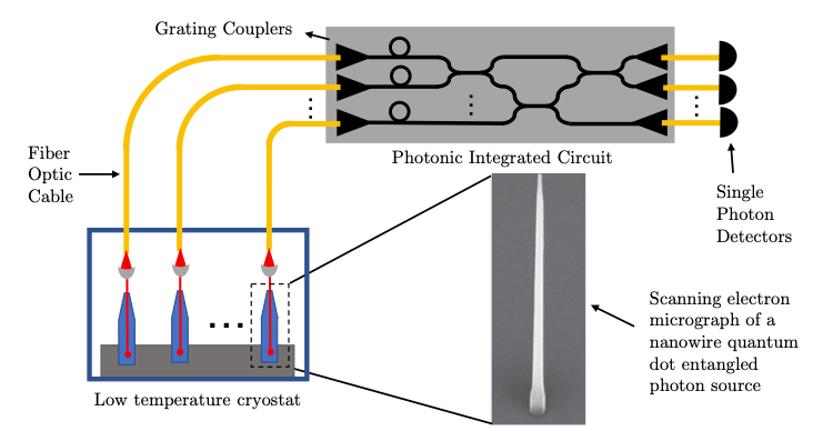
Figure 1. Illustration of the proposed experimental system for interfacing entangled photons emitted by the nanowire quantum dot sources with photonic integrated circuits for implementing quantum computing tasks on-chip. The emission from multiple entangled photon sources based on nanowire quantum dots that sit at low temperatures will be coupled to single-mode fibres. Using grating couplers, the entangled photons will be coupled into the photonic circuit for processing and then coupled out for detection.
Related Content

Harnessing the Promise of Quantum Materials for Future Electronic Devices
Summary Two-dimensional (2D) quantum materials, such as graphene and molybdenum disulfide, have great potential for use in future flexible and wearable electronics applications. With traditional silicon-based electronics nearing their theoretical performance limits, nano-electronics made from 2D quantum materials offer breakthrough opportunities for energy-efficient, wearable ubiquitous computation. In this project, we will study integration of […]
June 14, 2018

Metasurfaces for high-efficiency parametric downconversion and complex quantum state generation
Summary Entangled photon sources are crucial for quantum computing, quantum sensing, and quantum communication. Of growing importance are sources relying on spontaneous parametric downconversion (SPDC). Unfortunately, these sources of entangled photons are often constrained by momentum conservation laws. To overcome this limitation and expand the possibility of quantum state engineering, we intend to use metasurfaces […]
February 1, 2023
Folk Understanding of Quantum Physics
Summary It is often said that quantum concepts are counterintuitive. However, quantum concepts may not be equally counterintuitive to people from all cultural backgrounds. As cultural psychologists have discovered, culture fundamentally shapes the way people make sense of the world. In particular, the last few decades of research have documented cultural differences in appreciation of […]
March 24, 2021

Quantum Light Sources Based on Deterministic Photon Subtraction
Summary This project develops new sources of light that utilize quantum entanglement to enhance imaging resolution and detection. We aim to go beyond simple photon pairs and advance our understanding and control of new quantum states of light. Our approach uses deterministic single-photon subtraction (removing of a specific photon from a pulse of light) […]
July 13, 2018