TQT Transformative Quantum Technologies logo
  • En
  • Fr
Get Connected
TQT Transformative Quantum Technologies logo
Get Connected

"Find People, Projects, etc."

Generic selectors
Exact matches only
Search in title
Search in content
Post Type Selectors
job
publications
equipment
media
research
projects
people
events
labs
Filter by Categories
Committee
Leadership
Science
Staff
  • Home
  • Research
  • Opportunities
  • Events
  • About
  • Get Connected
  • Institute for Quantum Computing

    Scanning Tunneling Microscopy of Quantum Materials, Devices and Molecules

    Go Back Back

    More Topics

    0d 1d 2d characterization devices grand challenge materials molecules new ideas sensors spintronics STM storage transistor transport

    Summary


    This project advances our ability to characterize and study novel quantum materials, quantum devices, and even individual molecules at the atomic level. By combining Non-Contact Atomic Force Microscopy (NC-AFM), Scanning Tunneling Microscopy (STM) and scanning gate methods, we correlate spatial information with transport properties and can locally manipulate charge, spin and structural states. This opens a unique and useful window on the physics of 2D materials, 1D systems such as carbon nanotubes and 0D objects like quantum dots and molecules. We will collaborate with Adam Wei Tsen’s group to study surface electronic transport properties of 2D materials and correlate these with their bulk transport characteristics. We will also apply STM and Scanning Tunneling Spectroscopy (STS) to achieve atomic-scale resolution imaging of single molecules in collaboration with David Cory’s group. We expect this project will create a unique capability to probe and manipulate matter at the atomic scale, leading to accelerated development of novel transistors and spintronic devices, quantum sensors, ultra-high density classical and quantum information storage, and novel qubit applications.
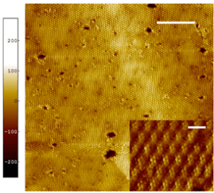
     

    Figure 1. Topographic image of exfoliated 1T-TaS2 at 77 K (scale bar = 20 nm) obtained in the scanning tunneling microscope. The colour scale is in picometers. The periodic structure resolved in the main image is a charge density wave known to occur in this material. Inset: magnified image showing both the charge density wave and the underlying atomic lattice (scale bar = 1.4 nm).

    Principal Investigator (PI) or Team Coordinator

    Jonathan Baugh

    sidebar icon sidebar icon sidebar icon sidebar icon

    Share

    • Share on Twitter
    • Share on Facebook
    • Share on LinkedIn

    Related Content

    Quantum Sensing Applications using Quantum Communication Technology

    Summary   The Quantum Encryption and Science Satellite provides a platform to develop and deploy quantum sensing and metrology via photonic channels. This project will build upon ‘free-space’ quantum communication technology and explore new approaches and methods to advance two primary applications: quantum-enhanced telescopes, and spectroscopic sensing for methane detection in the atmosphere. For the […]

    December 8, 2018

    PI: Thomas Jennewein

    Skip Tags communication grand challenge + 7 Additional

    • Share on Twitter
    • Share on Facebook
    • Share on LinkedIn
    • Go to Quantum Sensing Applications using Quantum Communication Technology
    Quantum Simulation of Strongly Coupled Field Theories
    TQT Computation

    Quantum Simulation of Strongly Coupled Field Theories

    Strongly-coupled field theories describe both fundamental and applied quantum problems.

    August 10, 2017

    PI: Chris Wilson

    Skip Tags computation electrical & computer engineering + 3 Additional

    • Share on Twitter
    • Share on Facebook
    • Share on LinkedIn
    • Go to Quantum Simulation of Strongly Coupled Field Theories
    Quantum Sensing with Small Quantum Systems
    TQT Sensing

    Quantum Sensing with Small Quantum Systems

    Summary   There are small quantum systems over which we have very good control and which have long lifetimes. Examples include the phosphorous (P) defect in silicon (Si) and the nitrogen vacancy (NV) defect in diamond. With P defect in Si, we focus on improving our understanding of the hyperpolarization mechanism to better enable engineering of […]

    December 1, 2016

    PI: David Cory

    Skip Tags chemistry grand challenge + 6 Additional

    • Share on Twitter
    • Share on Facebook
    • Share on LinkedIn
    • Go to Quantum Sensing with Small Quantum Systems
    Towards large area, resonant quantum tunneling diodes by continuous Langmuir transfer of exfoliated 2D materials
    TQT Communication

    Towards large area, resonant quantum tunneling diodes by continuous Langmuir transfer of exfoliated 2D materials

    Summary  Atomically thin 2D materials constitute promising building blocks for quantum devices due to their exotic, layer-dependent electronic properties. The ability to stack these materials in alternating layers enables heterostructures to be built in almost limitless combinations and over small enough length scales to observe quantum phenomena. So far though, practical implementation of devices based […]

    April 1, 2020

    PI: Michael Pope

    Skip Tags 2D chemical engineering + 11 Additional

    • Share on Twitter
    • Share on Facebook
    • Share on LinkedIn
    • Go to Towards large area, resonant quantum tunneling diodes by continuous Langmuir transfer of exfoliated 2D materials

    Connect with Us

    Join us at the frontier of quantum technology development. Request a visit, explore opportunities, and stay informed.

    Get Connected
    TQT Logo
    First Canada Logo
    • twitter icon
    • facebook icon
    • youtube icon
    • Home
    • Research
    • Opportunities
    • Events
    • About
    • Get Connected
    • Institute for Quantum Computing
    TQT Logo
    • Home
    • Research
    • Opportunities
    • Events
    • About
    • Get Connected
    • Institute for Quantum Computing
    • twitter icon
    • facebook icon
    • youtube icon
    First Canada Logo
    TQT Logo
    • twitter icon
    • facebook icon
    • youtube icon
    • Research
    • Overview
    • Updates
    • Projects
    • Publications
    • Labs
    • Quantum Innovation Cycle
    • Opportunities
    • Overview
    • Quantum for Health Design Challenge
    • Quantum for Environment Design Challenge
    • Quantum Seed
    • Technology Development
    • Open Positions
    • Events
    • All Events
    • About
    • Overview
    • People
    • Media
    • Contact
    First Canada Logo