
Summary
Atomically thin 2D materials constitute promising building blocks for quantum devices due to their exotic, layer-dependent electronic properties. The ability to stack these materials in alternating layers enables heterostructures to be built in almost limitless combinations and over small enough length scales to observe quantum phenomena. So far though, practical implementation of devices based on layered 2D materials has been limited by the challenges of depositing or transferring single atomically thin layers over large areas and of building multi-layers from different materials. In this project, we expand on our previously demonstrated scalable deposition techniques of films for electrochemical applications and control of defects in exfoliated 2D material flakes to build electronic and optoelectronic-based quantum devices in collaboration with Prof. Na Young Kim’s group. Our central goal is to create large area heterostructures of 2D materials built by sequential Langmuir-Blodgett (LB) deposition. We will use these heterostructures to construct simple proof-of-principle quantum devices such as resonant tunneling diodes (RTDs). The work will include finding optimized film parameters for dense, ultrathin tunneling barriers, development of patterning approaches compatible with sequential LB deposition, and ultimately demonstrating a working single, double, and multi-junction RTDs on flexible substrates. While the RTD is one of the simplest quantum devices that can be fabricated from heterostructures of 2D materials, the methodologies we establish in this project will pave the way for improved THz emitters and detectors, faster transistors and memories, and other devices that rely on similar heterostructures and design.

Figure 1. Large-area, atomically thin coatings of 2D materials prepared by continuous Langmuir deposition. Scanning electron microscopy image (top); Picture of large area coating on glass (bottom).
Related Content

Hybrid Quantum Repeater based on Atomic Quantum Memories and Telecom Wavelength Entangled Photon-Pairs Generated from Semiconductor Nanowires
Summary Losses in physical channels, such as optical fibres, limit existing quantum communication systems to modest distance ranges. Since amplification of quantum signals is fundamentally not possible, we look to extend the range and functionality of these quantum channels by adding quantum memory nodes that can daisy-chain multiple lengths of quantum channels through entanglement […]
October 29, 2018

Next Generation Quantum Sensors
We are developing new semiconductor p-n junctions and designing novel nanowire arrays that have the potential to significantly enhance the ability to detect light at the single photon level over an unprecedented wavelength range from the ultraviolet to infrared.
June 1, 2017
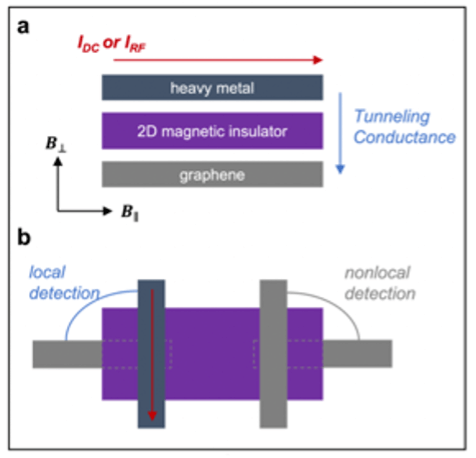
Coherent magnon generation, magnon condensation, and quantum spin liquids via spin pumping in 2D magnets
Summary Developing hybrid quantum systems is essential to harnessing the complementary advantages of different quantum technology platforms. This necessitates the successful transfer of quantum information between platforms, which can be achieved, e.g., by harnessing magnons, or spin wave excitations, in magnetic materials. Decoherence due to uncontrolled coupling of qubits to the environment remains a fundamental […]
February 1, 2023

Quantum Sensing with Small Quantum Systems
Summary There are small quantum systems over which we have very good control and which have long lifetimes. Examples include the phosphorous (P) defect in silicon (Si) and the nitrogen vacancy (NV) defect in diamond. With P defect in Si, we focus on improving our understanding of the hyperpolarization mechanism to better enable engineering of […]
December 1, 2016