
Summary
Scaling solid-state quantum processors to a useful threshold while maintaining the requisite precision in quantum control remains a challenge. We propose a quantum metal-oxide-semiconductor (QMOS) architecture operating at cryogenic temperatures that is based on a network/node approach as a means to scalability. By working with QMOS, we benefit from the deep investments and advances that have been made in conventional CMOS device processing, and natural compatibility with CMOS integration. The architecture uses one of the most promising error correction schemes: topological stabilizer codes acting on a two-dimensional qubit arrays, also known as surface codes. The network/node approach is advantageous because it separates the surface code operation into two fundamental parts: local node operations involving a handful of qubits, which should be feasible to demonstrate in the near-term, and medium range entanglement distribution based on electron shuttling, which is challenging but can be developed in parallel. A major focus of this project is to simplify QMOS devices – reducing the number of gate electrodes per device, even down to a single electrode. The team led by Dr. Baugh with collaborators Dr. Lan Wei and Dr. Michel Pioro-Ladrière combines expertise in electrical engineering and CMOS integrated design, QMOS fabrication and physics. By testing the viability of a network/node approach, this project charts a path toward a large-scale quantum information processor in silicon.
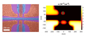
Figure 1. (left) A false-colour scanning electron microscope image of two metal-oxide-semiconductor (MOS) quantum dots, where one is placed as the mirror image of the other. Purple represents SiO2/Si, blue represents the aluminum screening gates, and red represents the aluminum accumulation gates. In this simplified design, the tunnel coupling between the dot and the source/drain reservoirs is controlled by the physical gap between metal gates and the voltage applied to the source/drain accumulation gates. (right) Nextnano simulation of the charge density in the silicon two-dimension electron gas with top gate voltages typical of device operation. Here, the lower device is used as a charge sensor (single electron transistor) to readout the charge state of the upper dot, which can be tuned to single electron occupancy to host an electron spin qubit.
Related Content

Rydberg Atom Array Quantum Simulator
Summary Quantum simulators enable probing the static and dynamic properties of correlated quantum many-body systems that would otherwise be numerically inaccessible using classical simulators. We are developing quantum simulators based on arrays of neutral atoms excited to Rydberg states. Such Rydberg atom arrays are advantageous for simulating the dynamics of interacting spin systems (Ising spin […]
February 27, 2020

Topological Quantum Computing on Majorana Platform
Full-scale quantum computing will require the capability for error-tolerant quantum information processing.
January 11, 2017

Quantum Information Processing with Molecular Lattices
The aim of the work is to develop theoretical tools to simulate and predict the behaviour of a one-dimensional chain of trapped dipolar molecules and to study the nature of entanglement as a design resource.
June 1, 2017

Cryo-CMOS to Control and Operate 2D Fault-Tolerant Qubit Network
Summary Large-scale, fault-tolerant quantum computation requires precise and stable control of individual qubits. This project will use complementary metal-oxide-semiconductor (CMOS) technology to provide a cost-effective scalable platform for reliable and high-density control infrastructure for silicon spin qubits. We will use sub-micron CMOS technology to address device and circuit-level challenges and explore the integration of […]
June 14, 2018