Summary
Two-dimensional (2D) layers just one atom thick can be stripped from certain materials, such as graphene. The individual layers from one or more of these materials can then be restacked to create cage-like quantum heterostructures, which possess novel quantum properties. Incorporating magnetism into such a structure at room temperature could enable direct control of electron spin polarization in the transistor geometry. We are working to combine 2D semiconductors and magnetic insulators as an early step toward creation of magnetic semiconductor heterostructures for spintronic devices. Along with proving the heterostructure concept, success in combining the two materials supports a subsequent goal, fabrication of a nanostructure consisting of a superconductor, semiconductor, and magnetic insulator. Achievement of these two goals will provide a fundamental building block for spintronics, address a vital materials challenge in the pathway to quantum computing, and potentially allow for integration of processing and storage technologies in a single device platform.

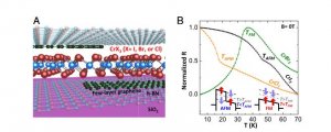
Figure 1. Magnetic van der Waals tunnel junction incorporating ultrathin chromium trihalides. (A) Schematic illustration of the device. (B) Normalizedtemperature-dependent dc resistance of CrX3(X=I, Br, and Cl) at constant current of 0.1 nA.Insetsshow schematics of the spin-dependent tunnel barrier forAFM and FM interlayer coupling. Red and blue arrows indicate spin orientation and are used throughout. Original illustration from PNAS Publications.
Related Content

Quantum Material Multilayer Photonic Devices and Network
Summary Realizing highly integrated quantum photonic devices on a chip can enable new opportunities for photonic quantum computation. In this project, we explore heterostructures of stacked two-dimensional (2D) materials, such transition metal dichalcogenides (TMDC) or graphene, combined with optical microcavities as a platform for such devices. 2D materials are extremely thin and flexible, and have […]
December 12, 2019

Distributing Multimode Entanglement with Microwave Photons
Microwaves have enabled numerous classical technologies, in part because they propagate through air with little energy loss.
March 6, 2017

On-Chip Microwave-Optical Quantum Interface
Summary In this project we develop a quantum interface between microwave and optical photons as a key enabling technology of a hybrid quantum network. In such a network, the robust optical photons carry quantum information through optical fibres over long distances, while superconducting microwave circuits protected from thermal photon noise by the low temperature […]
October 29, 2018

A Reformulation of Quantum Game Theory
Summary Classical game theory – conducted at the interface between economics and computer science – has found applications in topics ranging from networking and security to online markets. Despite over 20 years of research into connections between game theory and quantum information, we have yet to see any significant implications of quantum information when applied […]
April 1, 2020

