
Summary
Large-scale, fault-tolerant quantum computation requires precise and stable control of individual qubits. This project will use complementary metal-oxide-semiconductor (CMOS) technology to provide a cost-effective scalable platform for reliable and high-density control infrastructure for silicon spin qubits. We will use sub-micron CMOS technology to address device and circuit-level challenges and explore the integration of classical CMOS and quantum computing components. Since spin qubit control and measurement requires CMOS to operate at milli-Kelvin temperatures – far below the normal operating range of classical electronic devices – we will develop and calibrate compact models for MOSFETs at cryogenic temperatures, considering electrical, thermal and noise behaviors. These models will be used for cryo-CMOS design for spin qubit control operations, data readout, and communication, in a compact and scalable way at the node level. We hope to eventually implement integrated, readily scalable spin qubit control systems by bridging the classic CMOS and quantum platforms.
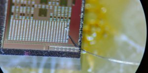
Figure 1. 65nm test chip for cryogenic device characterization
Related Content

Topological Properties of Exciton-Polaritons in a Kagome Lattice as a Solid-state Quantum Simulator
Summary In this project, we build a solid-state quantum simulator for engineering a specific Hamiltonian. Quantum simulators are purpose-built devices with little to no need for error correction, thereby making this type of hardware less demanding than universal quantum computers. Our platform consists of exciton-polariton condensates in multiple quantum-wells sandwiched in a semiconductor Bragg […]
December 8, 2018

Next Generation Quantum Sensors
We are developing new semiconductor p-n junctions and designing novel nanowire arrays that have the potential to significantly enhance the ability to detect light at the single photon level over an unprecedented wavelength range from the ultraviolet to infrared.
June 1, 2017

Spin Generation and High-Frequency Detection via the Quantum Nonlinear Anomalous Hall Effect in Weyl Semimetals
In magnetic conductors, the passage of current yields an electric field in the transverse direction even without an external magnetic field – this is known as the anomalous Hall effect (AHE). This effect can act as a convenient probe of spin ordering, magnetic textures, spin-orbit coupling, and band topology in solids, and can be further […]
April 19, 2023

Entangled Photon Orbital Angular Momentum Arrays
Summary Arrays of orbital angular momentum (OAM) states of light are a new form of structured light so far relatively unexplored in quantum information science. Unlike spin angular momentum of light, which is related to light’s polarization and covers two dimensions, OAM states, sometimes described as ‘donut beams’ due to the shape of the field […]
September 19, 2019