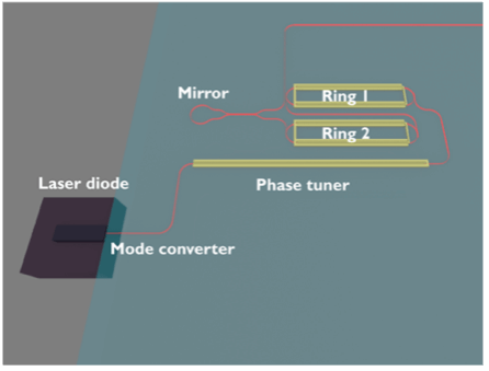
Atoms can be controlled by manipulating their internal states using agile, quiet and reliable laser sources. An external-cavity diode laser (ECDL) is a crucial enabling technology to realize such laser sources since it allows for the narrowing of the linewidth of a laser diode and precise tuning of the laser frequency. This project aims to miniaturize the external cavity using a photonic integrated circuit (PIC) (i.e., a single chip), which will increase the reliability and functionality of the optical frequency source for quantum experiments. A PIC ECDL will be designed and fabricated using aluminum nitride (AlN). Since several atomic transitions of interest in quantum applications are in the visible spectrum, AlN is an ideal material due to its large bandgap that allows for low-loss waveguide propagation. AlN also enables key functionality for preparing narrow linewidth and agile optical frequencies. Thus, an AlN waveguide will be fabricated and tested to ensure low waveguide losses at visible wavelengths. An external cavity feedback laser will be fabricated by coupling a laser diode directly into the AlN waveguide. A micro-ring resonator feedback circuit will be used to select and narrow the laser output. The light will be further coupled into fibre optics for delivery to atoms in a vacuum chamber, demonstrating the viability of using PIC ECDLs to interact with atomic energy levels. This AlN PIC ECDL would be a compact optical frequency source that could help enhance existing quantum experiments, enable experiments currently unviable with bulk optical setups and allow for the translation of quantum atomic technologies out of the laboratory (i.e., large-scale quantum computation, high-precision gravimeters for resource mapping and portable optical atomic clocks).

Figure 1. A conceptual render of an external cavity diode laser in an aluminum nitride integrated photonic circuit.
Related Content

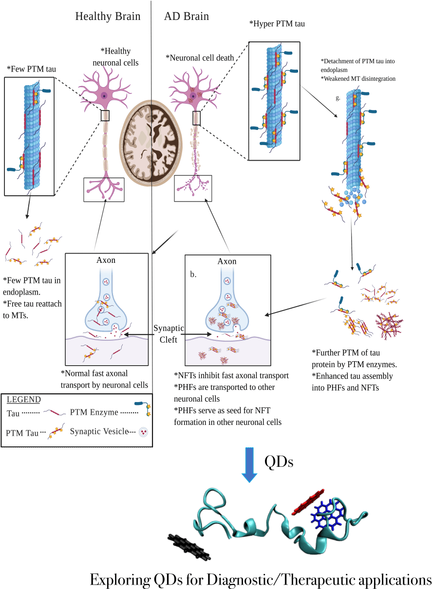
Identifying the Potential of Quantum Dots to Detect and Disrupt Tau Protein Aggregation in Alzheimer’s Disease
Specific tests for Alzheimer’s disease (AD) diagnosis are currently unavailable, despite AD being the leading cause of dementia. One hallmark of AD progression is the aggregation of tau proteins into paired helical filaments and neurofibrillary tangles, which is accelerated by the hyperphosphorylation of Tau proteins. However, the mechanism by which the hyperphosphorylated tau accelerates protein […]
March 27, 2023

Metasurfaces for high-efficiency parametric downconversion and complex quantum state generation
Summary Entangled photon sources are crucial for quantum computing, quantum sensing, and quantum communication. Of growing importance are sources relying on spontaneous parametric downconversion (SPDC). Unfortunately, these sources of entangled photons are often constrained by momentum conservation laws. To overcome this limitation and expand the possibility of quantum state engineering, we intend to use metasurfaces […]
February 1, 2023

Extensible Technology for a Medium-Scale Superconducting Quantum Processor
Summary Superconducting quantum bits, or qubits, use circuits made from superconducting materials to harness quantum mechanical states. These devices contain many atoms, but can behave as simple, controllable qubits. We are building technologies for the control and measurement of superconducting qubits to enable the first demonstration of an extensible, medium-scale quantum processor. Our approach […]
November 28, 2016


