
Summary
Two-dimensional (2D) quantum materials, such as graphene and molybdenum disulfide, have great potential for use in future flexible and wearable electronics applications. With traditional silicon-based electronics nearing their theoretical performance limits, nano-electronics made from 2D quantum materials offer breakthrough opportunities for energy-efficient, wearable ubiquitous computation.
In this project, we will study integration of 2D material electronic devices with ferroelectric (FE) layers to simultaneously achieve low-power and high-speed devices through material and design optimization. Using density functional theory (DFT) calculations, we will select optimal 2D materials for use in the active channels of transistors and develop models to describe the intricate physics of negative capacitance field-effect transistors (NC FETs) based on the FE-dielectric-2D material heterostructure. In the end, the project will develop a numerical simulation tool for 2D material NC FETs and verify our simulations through collaboration with experimental groups.
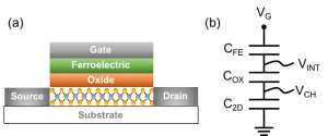
Figure 1. (a) A schematic of a 2D negative capacitance FET and (b) its equivalent capacitance network in equilibrium (VD = 0 V).
Related Content

Quantum Simulations of Fundamental Interactions
Summary To address questions in modern physics such as “what is the structure of matter inside neutron stars?” we need better computational methods to evaluate the interplay of fundamental forces between elementary particles. To-date the response to such questions rests on numerical computer simulations that are inherently limited. In this project, we develop new theoretical […]
April 18, 2019
Photonic Quantum Processor
Photonic quantum processors based on integrated quantum photonic circuits require entangled photon pairs to perform quantum computations. However, current state-of-the-art technologies utilize probabilistic entangled photon sources with limited pair-extraction efficiencies, negatively affecting the computation speed. This project aims to boost the speed of on-chip quantum operations by using bright, on-demand entangled photon sources with an […]
April 24, 2023

Topological Properties of Exciton-Polaritons in a Kagome Lattice as a Solid-state Quantum Simulator
Summary In this project, we build a solid-state quantum simulator for engineering a specific Hamiltonian. Quantum simulators are purpose-built devices with little to no need for error correction, thereby making this type of hardware less demanding than universal quantum computers. Our platform consists of exciton-polariton condensates in multiple quantum-wells sandwiched in a semiconductor Bragg […]
December 8, 2018

Developing Tools for Quantum Characterization and Validation
Summary Coherence is essential for quantum computation; yet it introduces a unique sensitivity to any imperfections in hardware design, control systems, and the operating environment. Overcoming these sensitivities requires a hierarchy of strategies, ranging from optimization of the hardware architecture to software solutions including quantum error correction. Randomized Benchmarking Protocols are an important family of […]
October 3, 2017