
Summary
This project advances our ability to characterize and study novel quantum materials, quantum devices, and even individual molecules at the atomic level. By combining Non-Contact Atomic Force Microscopy (NC-AFM), Scanning Tunneling Microscopy (STM) and scanning gate methods, we correlate spatial information with transport properties and can locally manipulate charge, spin and structural states. This opens a unique and useful window on the physics of 2D materials, 1D systems such as carbon nanotubes and 0D objects like quantum dots and molecules. We will collaborate with Adam Wei Tsen’s group to study surface electronic transport properties of 2D materials and correlate these with their bulk transport characteristics. We will also apply STM and Scanning Tunneling Spectroscopy (STS) to achieve atomic-scale resolution imaging of single molecules in collaboration with David Cory’s group. We expect this project will create a unique capability to probe and manipulate matter at the atomic scale, leading to accelerated development of novel transistors and spintronic devices, quantum sensors, ultra-high density classical and quantum information storage, and novel qubit applications.

Figure 1. Topographic image of exfoliated 1T-TaS2 at 77 K (scale bar = 20 nm) obtained in the scanning tunneling microscope. The colour scale is in picometers. The periodic structure resolved in the main image is a charge density wave known to occur in this material. Inset: magnified image showing both the charge density wave and the underlying atomic lattice (scale bar = 1.4 nm).
Related Content
Photonic Quantum Processor
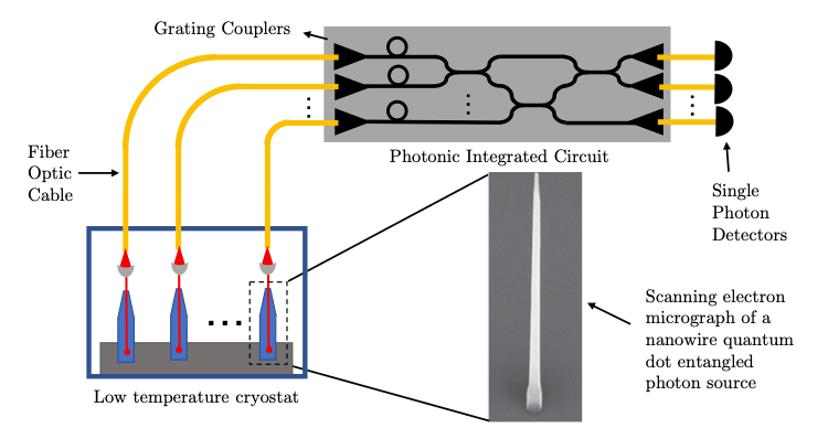
Photonic quantum processors based on integrated quantum photonic circuits require entangled photon pairs to perform quantum computations. However, current state-of-the-art technologies utilize probabilistic entangled photon sources with limited pair-extraction efficiencies, negatively affecting the computation speed. This project aims to boost the speed of on-chip quantum operations by using bright, on-demand entangled photon sources with an […]
April 24, 2023

Quantum Dynamics of Cavity Interactions with Spin Ensembles
Summary High quality factor cavities can be powerful control elements for ensembles of spins, enabling unitary control as well as on demand cooling. They can also be used to couple two otherwise non-interacting ensembles. The goal of the project is to explore the physics and engineering of such systems both theoretically and experimentally. The laboratory contains a […]
September 7, 2016
Structured Light Applications in Vision Science
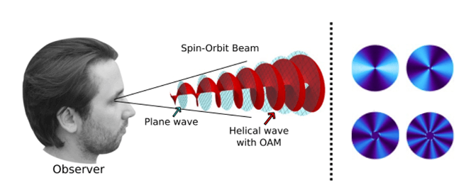
Eye diseases such as macular degeneration can have a devastating impact on quality of life. Early detection and treatment are thus crucial for preventing irreversible vision loss. A previous study found that the human eye can detect differences in ‘structured’ light beams. Such light beams are composed of a coherent superposition of differently polarized planar […]
April 24, 2023

Chiral Quantum Antenna Based on Multilayer Metasurface
Summary Individual atoms can act as stationary qubits and thus serve as nodes in quantum computing networks or as memories for quantum repeaters. However, to successfully use qubits based on single atoms suspended in free space, photons emitted by a single atom need to be efficiently collected. Conventionally, this can be done with high […]
September 20, 2018