
Summary
Individual atoms can act as stationary qubits and thus serve as nodes in quantum computing networks or as memories for quantum repeaters. However, to successfully use qubits based on single atoms suspended in free space, photons emitted by a single atom need to be efficiently collected. Conventionally, this can be done with high numerical aperture lenses, which can collect light from a large solid angle. Alternatively, placing the atom into a high-finesse cavity or within a sub-wavelength distance from the surface of a nano-photonic structure can affect the spatial pattern in which the atom emits photons and make the photon collection more efficient. However, these approaches remain experimentally challenging and can limit the potential for realistic scalability.
This project aims to achieve a distinctly novel way to control the emission pattern of a single atom by placing the atom at a distance of a few wavelengths from a chiral metasurface — a phased two-dimensional array of nano-scale metallic antennas or dielectric scatterers. We design and fabricate bi- and multi-layer structures with properly tuned interference between the radiation patterns of the layers. In the vicinity of such structures, the atom will emit light into a single, well defined direction without the need to place the atom at a sub-wavelength distance from a metallic or dielectric surface. The unidirectionally emitted photons can be efficiently coupled into optical fibers. Relative to current state-of-the-art, this platform simplifies and enables speed-up for certain quantum information processing tasks, such as remote entanglement between two distant atoms.
Simultaneously we will explore – through design and fabrication – the use of chiral metasurfaces for photon extraction from solid-state quantum emitters, such as colour centers in diamond. Here we hope to achieve increased photon collection efficiency from materials with high refractive index, which holds promise for improving the performance (speed and sensitivity) of electric and magnetic field sensors.

Figure 1. The spatial emission pattern of an atom suspended above the tip of an optical fibre is controlled by the two-layer metasurface mounted on the fiber tip. This allows efficient collection of the photons emitted by the atom and their coupling into the fibre.
Related Content
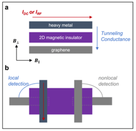
Coherent magnon generation, magnon condensation, and quantum spin liquids via spin pumping in 2D magnets
Summary Developing hybrid quantum systems is essential to harnessing the complementary advantages of different quantum technology platforms. This necessitates the successful transfer of quantum information between platforms, which can be achieved, e.g., by harnessing magnons, or spin wave excitations, in magnetic materials. Decoherence due to uncontrolled coupling of qubits to the environment remains a fundamental […]
February 1, 2023

Combined momentum- and real-space photoelectric probes of dimensionality-tuned Weyl semimetals
Summary The library of two-dimensional (2D) materials has recently grown to include topological insulators and semimetals. Their incorporation in special device geometries may lead to novel quantum electronics with enhanced functionalities. Weyl semimetals, in particular, offer the most robust form of topological protection. Recent results from our group indicate that Weyl nodes should be […]
March 12, 2019

Quantum Information Processing with Molecular Lattices
The aim of the work is to develop theoretical tools to simulate and predict the behaviour of a one-dimensional chain of trapped dipolar molecules and to study the nature of entanglement as a design resource.
June 1, 2017

Quantum Simulation of Strongly Coupled Field Theories
Strongly-coupled field theories describe both fundamental and applied quantum problems.
August 10, 2017