
Summary
Individual atoms can act as stationary qubits and thus serve as nodes in quantum computing networks or as memories for quantum repeaters. However, to successfully use qubits based on single atoms suspended in free space, photons emitted by a single atom need to be efficiently collected. Conventionally, this can be done with high numerical aperture lenses, which can collect light from a large solid angle. Alternatively, placing the atom into a high-finesse cavity or within a sub-wavelength distance from the surface of a nano-photonic structure can affect the spatial pattern in which the atom emits photons and make the photon collection more efficient. However, these approaches remain experimentally challenging and can limit the potential for realistic scalability.
This project aims to achieve a distinctly novel way to control the emission pattern of a single atom by placing the atom at a distance of a few wavelengths from a chiral metasurface — a phased two-dimensional array of nano-scale metallic antennas or dielectric scatterers. We design and fabricate bi- and multi-layer structures with properly tuned interference between the radiation patterns of the layers. In the vicinity of such structures, the atom will emit light into a single, well defined direction without the need to place the atom at a sub-wavelength distance from a metallic or dielectric surface. The unidirectionally emitted photons can be efficiently coupled into optical fibers. Relative to current state-of-the-art, this platform simplifies and enables speed-up for certain quantum information processing tasks, such as remote entanglement between two distant atoms.
Simultaneously we will explore – through design and fabrication – the use of chiral metasurfaces for photon extraction from solid-state quantum emitters, such as colour centers in diamond. Here we hope to achieve increased photon collection efficiency from materials with high refractive index, which holds promise for improving the performance (speed and sensitivity) of electric and magnetic field sensors.

Figure 1. The spatial emission pattern of an atom suspended above the tip of an optical fibre is controlled by the two-layer metasurface mounted on the fiber tip. This allows efficient collection of the photons emitted by the atom and their coupling into the fibre.
Related Content

Composite Superconductors for Improved Quantum Coherence
Summary Conventional superconductors have trouble performing well in magnetic fields required for electron spin resonance (ESR) – based quantum information processing applications. We can, however, use proximity engineering to select desired properties from different materials and combine them for improved superconducting performance in magnetic fields — an improvement that would have strong implications for […]
December 12, 2018
Fabrication of Ultra Low Noise RF SQUID Amplifiers
A superconducting quantum interference device (SQUID) is an extremely sensitive magnetic field detector.
June 1, 2017
Advanced microwave electronics enabling quantum technologies
Summary Superconducting quantum computers require quantum-limited measurements at microwave frequencies in order to implement error correction. Conventionally, this is accomplished using near quantum-limited Josephson Parametric Amplifiers (JPAs). The JPAs require bulky ferrite-based circulators that prevent on-chip integration of the amplifiers with the processor and take up the majority of space and cooling power in the […]
April 1, 2020
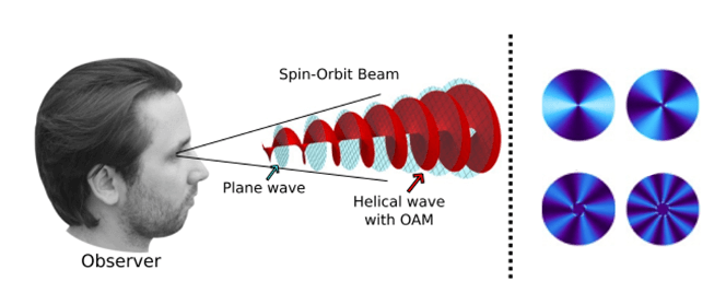
Structured Light Applications in Vision Science
Eye diseases such as macular degeneration can have a devastating impact on quality of life. Early detection and treatment are thus crucial for preventing irreversible vision loss. A previous study found that the human eye can detect differences in ‘structured’ light beams. Such light beams are composed of a coherent superposition of differently polarized planar […]
April 24, 2023