
Summary
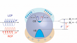
Thanks to the light-induced collective oscillations of free charges at the boundary between a conducting material and a dielectric, known as surface plasmon resonance, metallic nanostructures can exhibit strong light absorption and scattering. The sensitivity of these resonances to the local environment and shape of the metallic structures allows them to be used, for example, in chemical sensing and cancer therapy. Semiconductor and metal-oxide nanoparticles expand possible wavelengths of surface plasmon resonances into the infrared spectrum and can possibly allow for coupling of the surface plasmon resonances of the nanoparticle, which are of classical nature, to the particle’s semiconductor band structure, which arises from quantum states of the charge carriers. These charge carriers are the electron-hole pairs known as excitons in the semiconductor.
We have recently developed a new method to produce doped transparent-metal-oxide plasmonic nanocrystals and used these to demonstrate for the first time a plasmon-exciton coupling in any plasmonic semiconductor system. Our goal in this project is to further explore the plasmon-exciton coupling in semiconductor and metal-oxide nanostructures and to develop methods to use this coupling for plasmon control of the quantum states of single defects and for their entanglement. We expect this will open the door for these systems to be deployed in quantum sensing and computing applications. In particular, we believe our studies will lead to the design of inexpensive and highly sensitive magneto-optical sensors for thermal imaging and molecular sensing.
Related Content

Applications of Neutron Interferometry and Structured Neutron Beams
Summary Neutrons are a powerful probe of matter and physics due to their Angstrom size wavelengths, electric neutrality and relatively large mass. In this project, we develop quantum sensors that exploit these attributes to increases the precision of measurements of fundamental forces and materials structure. With David Cory, Alexander Cronin of the University of Arizona, […]
July 31, 2018

Zero-Dimensional Quantum Materials for the Next Generation of Highly-Selective Chemical Sensors
Summary Heavy metals are a major public health concern and their on-site detection in water supplies is not well served by existing lab techniques. We develop a new multi-modal platform comprising functionalized quantum dots of two-dimensional materials (2D-QDs) for the sensing of four highly-toxic heavy metal pollutants (arsenic, cadmium, lead and mercury). The zero-dimensional […]
March 11, 2019

Quantum Simulations of Fundamental Interactions
Summary To address questions in modern physics such as “what is the structure of matter inside neutron stars?” we need better computational methods to evaluate the interplay of fundamental forces between elementary particles. To-date the response to such questions rests on numerical computer simulations that are inherently limited. In this project, we develop new theoretical […]
April 18, 2019

A Reformulation of Quantum Game Theory
Summary Classical game theory – conducted at the interface between economics and computer science – has found applications in topics ranging from networking and security to online markets. Despite over 20 years of research into connections between game theory and quantum information, we have yet to see any significant implications of quantum information when applied […]
April 1, 2020