New device structure can improve the properties of integrated circuits towards low-power electronics
The development of a novel computational framework to investigate two-dimensional quantum material-based negative capacitance (NC) field-effect transistors (FETs) will enhance low-power electronics.
“Mobile electronics, such as smartphones and laptops, rely on low-power electronic devices. Prioritizing lower power consumption in the design of these mobile electronics increases the usage time between charges and reduces the amount of electricity needed to recharge them. However, designing low-power integrated circuits is challenging due to the growing demand for electronic devices, which are increasingly miniaturized with increased overall power consumption,” says Dr. Youngki Yoon, Associate Professor in the Department of Electrical and Computer Engineering and study lead.
To develop high-performing integrated circuits, field-effect transistors (FETs), which amplify or switch electrical signals, can be scaled down to fit more transistors on a single chip. Unfortunately, classical transistor technology is subject to Boltzmann’s tyranny, which limits subthreshold swing (SS). SS performance governs the behaviour of a transistor’s current-voltage characteristics when the transistor is switched on and off. A lower SS is desirable as it implies the transistor can be turned off with a smaller change in the applied gate voltage. Conventional transistors are limited by a minimum SS of 60 mV/decade at room temperature.
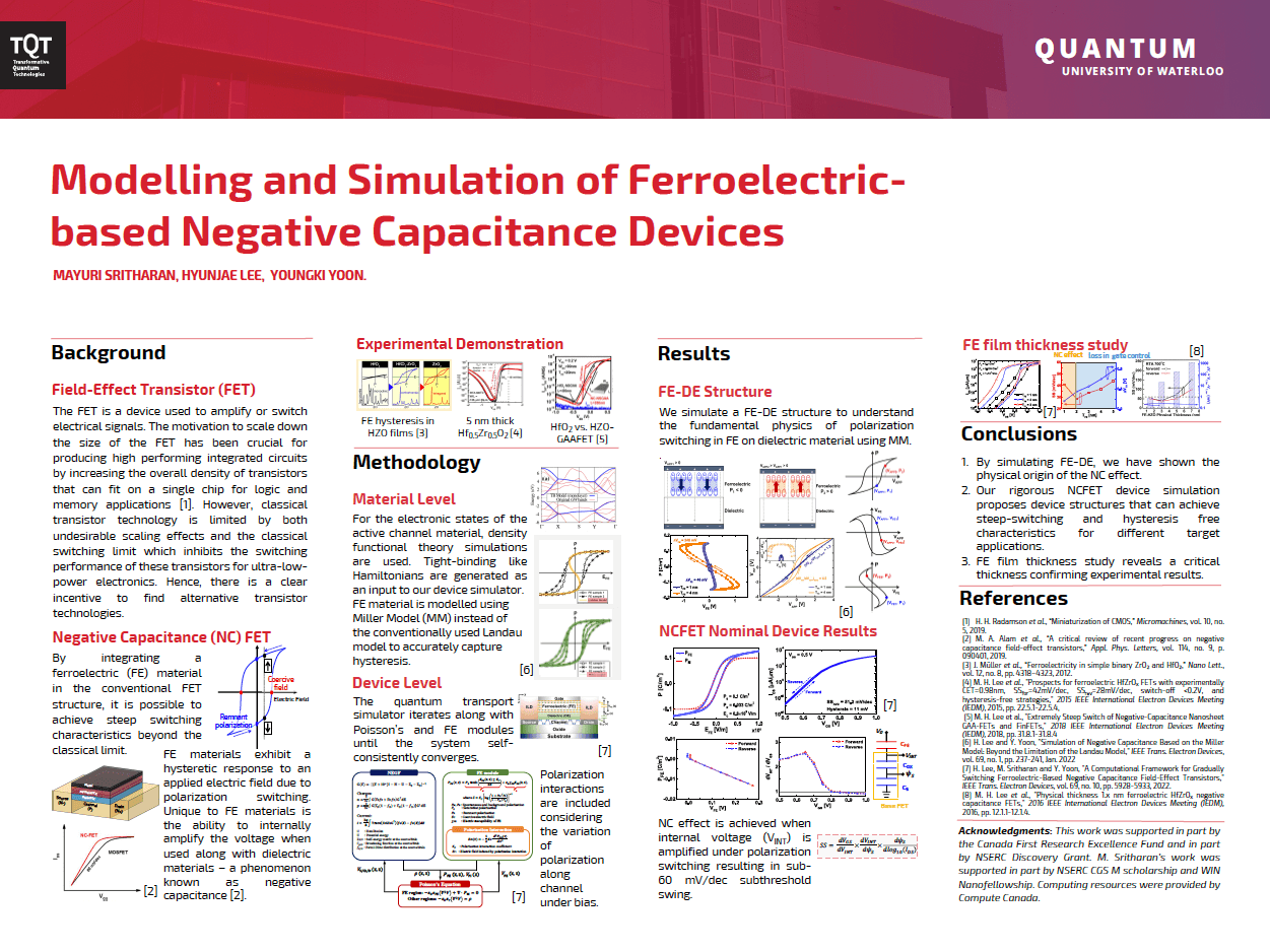
Expanding on work funded by a TQT seed fund, the researchers demonstrated that the classical limit can be overcome by integrating a ferroelectric (FE) material into conventional devices. When used with a dielectric (DE) material, the FE could internally amplify the voltage in a phenomenon known as the negative capacitance (NC) effect. Using a numerical device simulation, they explored an FE-DE bilayer and more intricate FET structures to understand the underlying physics of the polarization response of the ferroelectric layer. With this, they also elucidated the physical origin of the NC effect.
Based on the developed understanding of the underlying NC physics, a comprehensive NCFET device simulator tool was created. The proposed NCFET device was shown to overcome the fundamental limit in SS. By controlling the hysteric behaviour of the NCFET, researchers could also explore the potential of the NCFETs in different target applications. A hysteresis-free NCFET device can be used as complementary metal–oxide–semiconductor (CMOS) device for logic functions, allowing for low-power electronics with continuous scaling. Alternatively, an NCFET with a hysteretic response can be used as a non-volatile memory device to offer high endurance, non-destructive read, and low-power write for applications such as neuromorphic computing.
Although the work presented is simulation-based, other researchers experimentally demonstrated a critical FE thickness that can achieve the minimum SS with an NCFET device, confirming the theoretical results. With further optimization of the NCFET by tuning material and device parameters, future NCFETs can be designed for different applications. “The key insights delivered from our work help other researchers in our field make informed decisions towards the design and development of rarely explored electronic devices. Our research is important as it allows us to contribute to the advancement of transistor technology and next-generation computing.”
This research was undertaken thanks in part to funding from the Canada First Research Excellence Fund.
_____________________________________________________________________________________________________________________________________

Poster: Modelling and Simulation of Ferroelectric-based Negative Capacitance Devices
Poster authors: Mayuri Sritharan, Hyunjae Lee, Youngki Yoon
