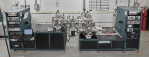
Thin Film Evaporation Sputter System
Provides thin films on chips using radio frequency (RF) and direct current (DC) sputtering methods, as well as molecular beam epitaxy (MBE). Able to grow most film substances on chips in high vacuum conditions.
Our AJA Thin Film Growth system uses radio frequencies (RF) to sputter semi-conducting and insulating materials on chips. The AJA system also deposits layers of conductors on chips using direct current (DC) sputtering. Both RF and DC methods are examples of sputtering methods to make amorphous, thicker layers. In addition to sputtering, our AJA system is capable of using molecular beam epitaxy (MBE), to grow multiple thin layers of materials. Sandwiched layers grown using MBE are made for research into topics like modern semi-conduction and semi-conducting chips.
Our AJA Thin Film Growth System is capable of growing oxides, alloys, pure metals, and more on chip substrates made of substances including sapphire, silicon, quartz, fused silica, and others.

